In the past 2 years, I was focus on the vintage multibit DAC (Digital to Analog Converter). I think all popular vintage multibit DAC IC has been use in my DAC project built. Those built are various in many different approach for each DAC section, solely to find what is the best variation among them.
I really like the sound characteristic coming from the vintage multibit DAC. For the example a complete audio system can be optimized in the sound quality by using a better source (media player). This what I found when I was a kid playing around making my own amplifier and speakers but when the same setups are using, and then I only changed the source from cassette tape to CD player, the sound quality was improving so much. The reason was because of the CD player specification are far superior than cassette tape. That finding was shocking me and then I keep continue to do the audition from many kind CD player that they are actually sound different one to another. Lately I was aware that the good sound quality CD player are mostly depend on what DAC use inside.
The vintage multibit DAC is an old technology. The latest is Delta Sigma DAC or anything they called it Bit-stream or 1 bit DAC are comes after it. Delta Sigma DAC is intended to contend the tolerance issue and the expensive production process of the vintage multibit DAC. But it cannot deliver the music lively compare to the vintage multibit DAC that sound more like human and musical. My love to the vintage multibit DAC are simply not for any nostalgic reason at all. I tried to convinced myself about today Delta Sigma DAC are better, but again, they never satisfy me to fulfilled my listening pleasure especially for realistic music performance experience.
In this post, I will explain my experience when building vintage multibit DAC.
Hope you enjoy this post and happy reading:)

A disclaimer for working on every electronic device will always need the basic skill to handle the components and working tools properly. This how-to explanation will not including in this post and the risk of doing it without proper skill will lead to personal injury or fatality. I believe you already have those skills before start to build anything related to electronic stuff especially any material stated in this post.
Do-it-yourself (DIY) electronic hobby is fun. When making an electronic stuff in general, the most common goal for every DIY in their first stages are aiming for the unit build to work properly. This is normal as their learning stages. But when the build are going more complicated and advance, the goals are more likely to compete with the target product in the same industry as close as possible.
One things should be bear in mind that DIY audio hobby will never be cheaper than bought.
This is not only for financial spending for the components and parts but the time consume to learn and build it is the factor to consider when dive into this hobby. Because this hobby is very addicted. So, please be aware:)
For myself, I like to make something that not only good inside, but it should be good in appearances just like professional built. I always called this progress is "building from nothing to something " and to be recognize as "this is different".
So I think I will make this special post by describing the concept behind my vintage multibit DAC built.
You may also treat this post as an entertainment only.
Especially if you already following my blog, you might enjoying my DAC building process, then this post might be your place to read the concept behind it. Also with all my thought from each DAC built are included.
Short brief about myself, I am an implementation person, I use the measurement, technical details and operating theory on each manufacturer datasheet as reference. When I want to build a DAC, I compare each datasheet and make a plan for it.
This might be a withdraw for someone looking for more technical details and measurement result of my DAC build. Sorry about that, I cannot provide those measurement since I am not using oscillator or any analyzer tools for my finished DAC built. I made them with one goal in mind is to deliver the best sound quality DAC at my listening chair.
As I said earlier, please take this post as an entertainment only. Make this post enjoyable for you to read and hopefully it inspire yourself for making something better than I was built here.
2. Where to Start?
The main components of the DAC is the DAC IC itself. I've post here about the tier list of vintage multibit DAC. It is a good way to start choosing the DAC IC that suitable for you to build.
All vintage multibit DAC are obsolete product. The manufacture already stop their production many years ago as well as their support to them. Easy solution get those DAC IC are by search and buy it online. But I not recommend this solution because it is quite risky especially if you don't really know the seller reputation, then the chance to get fakes components are huge.
The only source to get 100% authenticity DAC IC is taken directly from the used audio products. The example for CD player from year 80's to early 2000's are become my target to get those vintage multibit DAC IC. Some of them might broken already but probably only at the moving mechanism or on certain section that not effect to the main DAC components.
You might find this link useful. This can be your reference when looking for certain model CD player with specific DAC IC inside them.
Previously I've bought several CD player for my DAC build project and as far as I remember, they are: Clarion HX-D1, Clarion DRX9255EXL, Nakamichi DAC-101, Nakamichi DAC-41, Pioneer DEQ-P9, Pioneer Premier PD-93, Esoteric CDP (forget the model), Yamaha DAC DX-U1, EAD DAC-5000, Adcom GDA-600, Sinergetic Reasearch, KCD-55 Ultra, Marantz CD72, Denon CD (forget the model), Teac professional mixer (forget the mmodel), Madrigal Proceed CDP, Meridian DAC and many more.
Considering the large number collection above, for sure they are not easy to find.
I was not only take the DAC IC from those unit but the others useful components such as power transformers, heat sink, and op-amps are still worth to collect without any degradation issue. Unlike for the others components such as electrolytic capacitors, potentiometers, trim-pots, and resistor are the components that can be degrade when in use. So strictly to them, I always use the brand new components for the sake of reliability.
3. PCB Design & Layout
PCB is the base for the components to be placed on. Making a good PCB today can be done easily using computer. The designed files from the computer are send to the PCB maker and then they will start to build it using advanced technology in the PCB making process. I remember in the old days, when we want to make a pre-design PCB is by using the traditional way. A plain PCB with copper on top, then drawing the line using a masking film, then the PCB is heated and soaked into the chemical liquid.
Unfortunately I am not good at making PCB at all. I was never build it either using computer or in the traditional way. Then I start to do the electronic project by using point-to-point wiring on top of an universal PCB and keep enjoying to doing like this, continue until today. I think this is become my personal solution because I am lack in PCB making skill.
You saw already when I make my DAC are all using this point-to-point wiring method. You might wondering that this method is complex and probably problematic. But these are my thought about this method.
1. Designing the PCB using computer is still not an easy task. At least for me. This method is very useful when use for mass production. It will far be more efficient to the production line as well. But if it for personal use like I did here, then using a pre-design PCB it is completely waste of time.
2. The components that I use in my DAC build are often change based on the availability or any better quality replacement option. It is often for the components size are way bigger as my initial planning. This condition will become problematic on pre-design PCB because the format of the PCB are designed to dedicated components size only. Fortunately when using point-to-point wiring method, I could be more flexibility to use many components option for my built.
3. I never made one DAC twice. This is because I am still in the observation stages for this vintage multibit DAC. There will always any changes in my next DAC build. So doing in this point-to-point wiring method is more preferable.
4. Inter-component's joint quality when using in the point-to-point wiring, in my opinion are better compare to the pre-made PCB. I always use the high quality components because they have better quality material, not only for their main components material but also on their leads/ wires that I need to connect each others. Mostly the are using pure copper or silver wires. If I compare it to the pre-made PCB copper traces, I questionably the thickness and the quality of the copper that they are use in it.
5. The last reason to do this point-to-point wiring method is for fun:)

Then, what are the bad consequences when using this point-to-point wiring method?
1. Some said the DAC ground plane is very important to minimized the noise which I completely agree. For the example, the decoupling capacitor should be placed as close as possible to the each correspondences IC pin. The other decoupling capacitor pin are preferably connect to the ground plane as well. This method is a standard procedure when designing the components placement in the PCB.
2. It is hard to make any replacement or upgrade components with this point-to-point method especially when the initial components are already soldered into the board. Then if you insist to change them, this probably will damaging the PCB. Including extra work to realign the internal connection again.
3. There will probably an error when built a DAC in this point-to-point wiring method. I always spending more time to check each of the connection between components before starting the initial test. This to prevent any malfunction and error from the build.
So I think, this point-to-point wiring method will not friendly for the beginner. I have no other option since this method is more faster for me to start building the DAC.

4. Digital Receiver
Let's start to the main DAC built topic and the first stage is always about the digital receiver.
Digital receiver is where the digital signal from source are decode intentionally for the next stages DAC requirement. The reason for this decoding process is because all digital format are initially comes with the same data & clock in the single signal transfer. This digital connection is called SPDIF (Sony Philips Digital Interface) made for the consumer use. This SPDIF connection is use when they want to have a digital audio connection between the source to the external DAC. SPDIF is one of the very old digital connection that still in use today. It is basically a single RCA connector with coaxial cable in one end or using BNC connector with coaxial cable in the other end.
There are many digital connection cables besides the SPDIF. Instead using the electrical digital signal transfer in the SPDIF, the solution using the laser beam and optical connection are become popular as well. The most popular optical connection was invented by Toshiba and they called it Toslink connector. Naturally, this optical digital transfer can be faster and noise free compare to the SPDIF connection because of the isolation between the source to the DAC.
In this vintage multibit DAC digital receiver section, the digital audio format use is in PCM (Pulse Code Modulator). This PCM format are known as WAV, MP3, ALAC, FLAC audio files which they are widely use since the first time digital audio was introduced. The latest format in this audio industry is the PDM (Pulse Density Modulation) which they are actually made for SACD, a 1 bit audio processing either in DSD or DSF format. When using the PDM files for digital receiver on the vintage multibit DAC, the files should be convert to the PCM format first. This converting process should not become a problem since mostly the option is already included in the digital source that you are using right now.
Crystal CS8412 or CS8414
The most popular digital receiver for SPDIF or Toslink connection is using Crystal CS8412 or CS8414.
They are widely use in many DAC receiver for years, so finding this IC will not really hard to do. The CS8412 or CS8414 are both shared the same pin configuration and function which they can operate in stand-alone device without any external micro-processor control. Specifically for the CS8414 is the newer version compare to the older CS8412, capable to decode the digital signal up to 24 bit 96 kHz.
Going forward, I just say CS8412 to cover both model number.
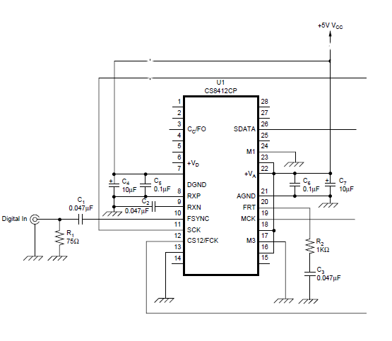
The simple schematic as shown bellow is for SPDIF connection to the CS8412 that can be done by using the RXP and RXN pin input. Thanks to the internal CS8412 that included the RS422 line receiver, so the external components around CS8412 can be minimized.
.png)
The function of the 0.01uF capacitors for each line receiver input (RXP Pin 9 & RXN Pin 10) are for isolation purpose from the source signal to the CS8412 digital receiver. The resistor function is to set the input impedance stay at 75 ohm.
Other connection method is by using digital isolation transformer. This is commonly use for the professional digital connector through AES/EBU balanced digital cable.
.JPG)
When using the Toslink optical connector, I simply use the schematic on their optical receiver datasheet. I using Toshiba TORX-176 optical receiver on my previous DAC built with good result. The output from the optical receiver is in TTL format and isolated already (because of the laser signal transfer mentioned before) then the use of 0.01 uF input capacitors to RXP and RXN as per CS8412 datasheet can be delete since they are not necessary.
The connection for TORX-176 are shown bellow.
.png)
The possibility to use more than one digital input, either SPDIF or Toslink can be done as per schematic bellow. It shown the JP1 is the jumper to selecting between those digital inputs. This jumper can be replace by using mechanical relay or passive switch or digital switch for the digital input selector.
.jpg)
After understanding the design of the digital input receiver, then the next step is to configure the CS8412 data output format. This section is very important since the data output format need to be carefully study and comparing between the digital receiver to the next DAC stages, either to digital filter or to non-oversampling DAC connection.
The reason CS8412 is very popular digital receiver because it has multiple digital format output. Those output format can be selected by configuring the combination between M0, M1, and M2 (except for the M3 is strictly to ground) as suggested in the datasheet.
.png)
As you can see from the table above, the combination of 1 and 0 for the M0, M1, M2 resulting several output data format.
In all of my DAC built project, I always use this popular data format:
1. Format 2 is I2s output (was invented by Philips) capable up to 24 bit digital data output. I2s format is more simple because it has fewer number of digital connection compare to others. When building the non-oversampling DAC using CS8412 with TDA1543 or TDA1541, the connection between digital receiver output to DAC IC input can directly connected because they are in the same I2s format.
2. Format 5 is 16 bit LSBJ output - MSB first data format. I often call this format is Sony Mode because all DAC IC besides made by Philips are all using this format.
3. Format 6 is 18 bit LSBJ output - MSB first, the same as above but different on the number of the bit output.
The example for CS8412 data output format configuration are shown on the schematic bellow. M0 to the ground and the M1 & M2 are tie to voltage pin VD+. This configuration resulting CS8412 into format 5 or 16 bit Sony mode.
For the CS8412 data output pins are follows
PIN 11 = FSYNC/LRCK
PIN 12 = FCK/BCK
PIN 26 = DATA
PIN 19 = Master Clock that strictly 256fs (will use only at Digital Filter section).
Using this CS8412 is my recommendation for the digital receiver in any DAC build. This is because of the data format output flexibility, minimal external components required and it come in DIP IC package, a through hole IC package that easy to handle by hands.
Yamaha YM3623 digital receiver
Yamaha YM3623 is more ancient digital receiver than the CS8412. At that time, it is a very popular digital receiver and use in many CD player until early 90's before the CS8412 start to replace it. The reason for this is because YM3623 require more external components to make it work. It require external oscillator circuit and it also require external line receiver for the digital input. For the data output format, this YM3623 can only deliver 16 bit LSBJ (Sony mode) output. This is because at that time, a 16 bit DAC is still new, the successor from more ancient 14 bit DAC.
For the DAC application that require more than 16 bit data output, this YM3623 still can be use but with using the Digital Filter multiple format output. The output from the digital filter are up-sampling with mostly above 16 bit output required to the newer DAC input format.
The YM3623 digital receiver is well know for it's higher jitter output performance compare to the CS8412. The jitter is basically an error in the digital signal, meaning when jitter present, the data transfer are partially corrupted and not exactly the same as the original. This jitter issue can cause lower sound quality and for the listener, this might be barely noticeably especially when there is no direct comparison between them. Jitter issue can be minimized by using separate jitter reducer circuitry that involving better clock, but this might be out of the topic right now.
So here is the schematic for YM3623 digital receiver.
.png)

The most popular digital audio connection right now is using USB (Universal Standard Bus). The source like PC, laptop, or smartphone with their music online or offline apps such as Foobar2000, UAPP, Spotify, Apple Music are more convenient to use. The USB is the only connection for their digital audio connection.
USB is a two way communication between source and receiver which in many cases, this might be problematic if the source or the receiver are so picky so they cannot detect the device correctly. I can recommend to use the most popular and trouble free USB digital receiver is the PCM2706 USB to I2s module. This module will work like charm with any device plug into it.
The downside is this PCM2706 is only processing 16 bit data output which anything above it will down-sample to 16 bit.

When I want more than 16 bit USB receiver then this is my recommendation.
The more advanced USB digital receiver is using XMOS U204 Altera Max USB to I2s module . This is more expensive than PCM2706 simply because it is capable to process the data up to 24 bit 192kHz through I2s output. This high bit USB receiver is still useless when pairing with any of the vintage multibit DAC because the highest bit rate is only on PCM1704 DAC IC capable up to 24 bit 96 kHz only.

Both PCM2704 or XMOS U204 USB receiver module are strictly I2s output.
The I2s digital connection only have 3 connection (excluding the ground) which are:
DATA for both right and left channel
BCK (bit clock)
WS (word clock)
Although one format can be convert to the others, but the benefit when using the I2s data format is actually more flexible to convert. For example if the DAC input data format requirement should be in the Sony format, then this I2s data can be convert easily using the serial hex inverter to specific bit in the Sony format. This topic will discuss on the non-oversampling section later in this post.
JL Sounds I2soverUSB module
Since the popularity using USB for audio connection are rose lately, the electronic engineer keep developing this technology aiming for more simple application yet better jitter performance. One of them is JL Sounds I2soverUSB. This module has greater flexibility to choose with so many data output format, not only in I2s output, but various Sony format from 16, 18, 20, and 24 bit output. So when building non-oversampling DAC, the connection between this USB digital receiver to specific DAC IC can be directly connected.

My thought when choose the Digital Receiver
I still use SPDIF connection for my digital receiver because I using digital audio player device that have the SPDIF output as well. I have my favorite CD's collection that I can easily converted to WAV files using the Exact Audio Copy, a PC program that by default convert the CD to the music files at 1,440 bps. Then I put those files in my SD card and play through my digital audio player which act as a digital signal transport.
I am prefer to use this simple setup to listen the music.
I am quite picky to choose the music that I want to hear and I am not a fans for searching and listen to the new songs or exploring the music collection on the online music provider library.
But perhaps it is just me.
Some said that the SPDIF connection is one way communication which (audibly) better than using a USB as the digital receiver. But I don't think so and I don't want you to choose the digital receiver based on this claim. I recommend to choose the digital receiver, either USB, SPDIF, or Toslink based on what your own preferable source instead. If you are using your smartphone to listen the music and you also want it to become your main digital audio source, than using the USB receiver is the great way to go.
5. Digital Filter & Non-oversampling
The next step after the digital receiver explanation above is when to use the digital filter (oversampling) or the non-oversampling method.
This topic is always debatable between when to use digital filter for over-sampling or not to using it. But before going to any of my conclusion, let me explain why we want to use the digital filter for the oversampling DAC.
Digital Filter (Oversampling DAC)
The main purpose for the digital filter present in the DAC is to recreate the data staircase on the digital domain based on it's internal digital signal processor. The result from this process is the data transition will be more complete and smoother. This proses resulting to what we know in the digital filter specification are: the number of taps, the stop-band rejection, digital filter ripple and the pass band response that always shown on each digital filter IC manufacture datasheet.
Digital filter is an advanced technology device. They just like a small computer but only for digital audio processing. The engineering understand that a 16 bit DAC will never have true 16 bit data processing because of the jitter issue or the accuracy of the multibit DAC structure. That is why in the digital filter, the sampling data input are commonly multiply by several times, far above the original files.
This is why we call this oversampling method when use in the DAC circuit.
Using digital filter is a very common practice in digital audio. Almost all CD player using this oversampling method. The goal when using this digital filter in the DAC is to get much more simple analog low-pass filter (LPF) design, resulting slower LPF cut-off and less passive components required.
Other than that, digital filter can be use as bridging between the different data from the receiver to the specific DAC data requirement.
Since the goal from this digital filter is direct effect to the overall DAC sound quality, so the quality from this digital filter should be always put as first priority. I've tested several digital filter IC and here are my recommendation:
SM5813APT
16 bit LSBJ digital input only, selectable data output 16 /18 /20 bit LSBJ, various master clock rate input, good sound quality and very popular digital filter IC easily get from old DAC unit.
DF1700
Basically same digital filter as SM5813APT but from different manufacture. SM5813APT pin compatible and no difference in the audio performance as well.
SM5847
Latest digital filter technology, various 16 /18 /20 /24 bit LSBJ data input & output, various master clock rate, comes in QFP small package that hard to work with bare hands and significant better audio performance than SM5813APT.
DF1704
It was made for 24 bit PCM1704 DAC, various 16/18/20/24 bit and I2s data input & output, comes in SSOP package and this is one of the best sound digital filter.
CXD1144
The most advanced digital filter in 90's with total 293 taps is the highest number digital filter at that era, 16 or 18 bit LSBJ data input format, I2s, 16 /18 bit LSBJ data output format, Master clock strictly on 384fs, the only dual parallel 22 bit processing system in one die and resulting the very smooth sound audio quality.
PMD100, PMD200
HDCD compatible, I2s input, various 16 /18 /20 /24 bit LSBJ data output, various master clock: 384fs or 256fs and one of the best sound quality when HDCD is locked.
.png)
.png)

When a DAC using high performance digital filter, it will give better audio measurement. The sound quality result would be more linear, cleaner, more precise, more specious sound-stage, more detail, smoother in all audible frequency response, and better depth and clarity.
This good result is what we want from our audio system right?
But the reality are not comes that easy. Especially when using the low quality digital filter concerning to more economical budget build, then the sound quality are become constrained in dynamic, probably sound boring and like an electronic toy.
The specific reason for digital filter IC are widely use in many CD player for years is for data bridging between DSP IC output that comes after processing from the compact disc then it convert by using this digital filter as bridging with the specific DAC IC. The other reason when using digital filter is to make the LPF analog section more simple and economical for CD player manufacture to build.
The purist audiophile assume when using digital filter is actually manipulating the original data. This thought is in my opinion correct since the digital filter function is to predict and add the data that actually not exist in the original.
Even though of those claims, I have successfully made few great sounding DAC using digital filter. One of them, which I really like is the CS8412 - SM5813APT - PCM63 DAC here is a great DAC with more like human voice reproduction, with more open sound-stage and detail sound characteristic. The other DAC built is when I use YM3623 - CXD1144 - AD1865 DAC here makes the sound characteristic very smooth, linier and clean in the audible frequency response.
Non-oversampling method
The reason why non-oversampling become more popular right now is because the simplicity of the connection between digital receiver to the DAC IC. They can directly connect each other without any digital filter in the middle as long as the data format are both the same. This method avoiding the complexity of digital filter configuration as explain above.
The non-oversampling DAC meaning that the data output from the digital receiver are connect directly to the DAC IC. There are no any re-sample and up-sample or data processing that many of us thought that using digital filter is manipulating the original data. This non-oversampling DAC only works for multibit DAC, in contrast for the Delta Sigma DAC, all data require to be up sampling first.
Things to consider from the nature of the non-oversampling DAC is the digital noise are greater, probably resulting poor audio measurement compare when using the digital filter. The impact to the sound quality is more raw, un-polished and lot of harmonic distortion.
Vice versa, the good non-oversampling DAC implementation will bring the music to live, more vocal presence with human like sound, great detail, imaging and sound-stage.
Direct I2s Non-oversampling
Using I2s data format for both digital receiver and DAC is the most simple non-oversampling DAC to build. You might revisiting my post here about the non-oversampling DAC built using TDA1543 DAC.
The connection from I2s digital receiver output to the I2s DAC input are configure like this:
LRCK --> WS
BCK --> BCK
DATA --> DATA
Vintage multibit DAC that are using I2s format input are strictly from Philips DAC. Their DAC are TDA1543 and TDA1541 only. Others than that are mostly using the Sony mode data format.
I have successfully built several non-oversampling DAC using TDA1541 with great result. They are here and here. The sound characteristic when using TDA1541 in the non-oversampling DAC is more raw sound presentation, more like the sound of records than digital but without missing the detail and dynamic.
Simple non-oversampling DAC using the Sony format
The vintage multibit DAC manufacture besides Philips are only Burr-brown (now Texas Instrument), and Analog Device which all of them using the Sony format.
Unlike the I2s data, the Sony format input DAC are more complex because it require to separate the data for left and right channel. The problem is on the digital receiver is only have one data output combine both left and right channel, controlled by the LRCK clock timing (or FSYNC as per CS8412 datasheet).
.png)
To understand this simple non-oversampling method, we also need to look at the DAC data input as shown on the AD1865 datasheet bellow.
AD1865 DAC IC is an example for the simple non-oversampling DAC implementation in the Sony format. This AD1865 is actually two 18 bit DAC in one package IC. Each channel have their own data input, shared the same LRCK clock timing. The data for left and right channel are separate at their own specific IC pins. This is the same with others DAC in this Sony format, either just like the AD1865 stereo DAC in one IC package or monotonic DAC IC which one DAC IC for one channel only.
.png)
The simple non-oversampling DAC method can be done by inverting the LRCK signal from the digital receiver output to the same DAC input data. The inverted LRCK will become the right channel and the non-inverted LRCK will be the left channel.
To simplify, this method using the same data for both DAC IC channel but LRCK timing control the portion for the right and left channel.
The others example for this simple non-oversampling DAC is shown on the PCM56 DAC schematic bellow. Two monotonic DAC IC with the same principal as the AD1865 DAC above but the digital receiver data output should be in the 16 bit Sony format when it pair with this PCM56 DAC IC.

This simple non-oversampling DAC are limited to the digital receiver data output only. For example the CS8412 only have 16 or 18 bit output in Sony mode, so the matching DAC are limited only for the 16 or 18 bit DAC such as: PCM56, PCM61, PCM58 or AD1865.
Higher bit number DAC, for the example 20 or 24 bit DAC such as PCM63, AD1862, PCM1702, or PCM1704 are cannot be use with this simple method anymore and they require more complex conversion using the serial shift register.
So with this limitation, this simple non-oversampling DAC is not perfect.
The others problem need to be addressed is because the 74HC04 hex inverter naturally delay the LRCK clock in few milli-second. The inverted LRCK data channel which is the right channel audio will also effect to this delay as well. This flaw might be arguable since the delay are so small and by adjusting the right channel speaker position closer to the listener probably will cure this delay problem. But if this simple non-oversampling method is intended to use with headphone, then it cannot be fix anymore since the headphone's drivers are both attach to the listener head.
I was successful made a great sounding DAC using this simple non-oversampling method here which consist of CS8412 - 74HC04 - 2 x AD1865 parallel. The sound quality is shockingly natural, great pin point imaging with lots of micro details.
More complex non-oversampling DAC using Sony mode
The idea when using the serial shift register circuitry is to convert the I2s data from digital receiver to specific bit require by specific DAC IC.
The shift register main components is using few 74HCT164 IC configure in series. They shift the I2s data to specific Sony data format either 18, 20 or 24 bit. This shift register circuitry is immune to the one channel imbalance like the simple method above.
The idea for this serial shift register schematic is taken from pavouk.org.
The example to shift the I2s data to 24 bit for PCM1704 DAC are shown on the schematic bellow. This circuit require 5 pcs of 74HCT164 in series to configure for right and left channel data.

For 18 bit data conversion is require six 74HCT in series. The schematic bellow is an example for AD1865 DAC.


Other non-oversampling method
The other non-oversampling method is using the JL Sounds I2sover USB digital receiver module.
This is smart USB module that can be configure easily with any specific DAC connected to it. The user manual explain clearly how to configure the output from this module with the schematic provided.

I had test this module on my previous non-oversampling DAC project before with the same result as when I using the series shift register above.
.png)
My thought when using the non-oversampling method
This non-oversampling approach are more easy to understand and also more easy to build. The components for this non-oversampling method are either using 74HC04 hex inverter or a series of 74HCT164 shift register, or the latest one is using JL Sounds I2soverUSB module.
The non-oversampling DAC sound characteristic are so much different with the digital filter oversampling DAC. With the same digital receiver and analog circuit, the non-oversampling DAC will sound warmer, more forward in the vocal, more live sound experience.
6. Digital to Analog Converter
This DAC section is the main discussion in this post.
How to configure this DAC are actually pretty simple to discus since their specific function is only converting the digital signal input to the analog signal output. To start with it, I shall recap every DAC stages that they are all contribute the overall sound quality.
I would say the digital receiver will contribute at least 10%.
Using digital filter or using non-oversampling method will contribute about 20 - 30%.
For the DAC IC will, it contribute at least 30% - 50%.
The Analog stages also has the great impact which about 20% - 40%
And the last is the power supply that take the rest of the percentage sound quality contributor.
Choosing the DAC IC
I would recommend to read my DAC tier list here because every DAC will always sound different if put in the same exact circuit.
The Philips vintage multibit DAC are strictly to TDA1540, TDA1541 and TDA1543 which are very popular in their own multibit system using active divider named Dynamic Element Matching (DEM) structure. This DEM is not resistor ladder DAC but shared the same working principal with the popular resistor ladder DAC.
The Burr-brown use resistor ladder DAC or what we often call it R2R DAC. Burr-brown vintage multibit DAC are various, start the oldest is PCM53, PCM54/55, PCM56 (the most popular), PCM58, PCM61, PCM63 (the best DAC), PCM1702, and PCM1704 (the last vintage multibit DAC).
The Analog Device came to this vintage multibit DAC game later on by mimicking the Burr-brown foot steps. Besides the AD1865 DAC, Analog Device product line up are similar to Burr-brown such as AD1860 (same as PCM56) and AD1862 (direct rival to PCM1702).
In the 20 bit DAC competition, the Analog Device DAC performance cannot compete anymore with the Burr-brown DAC. Then the Analog Device start to shifting to the Delta Sigma DAC while Burr-brown still making the vintage multibit DAC until PCM1704 that become their last 24 bit multibit DAC.
I take an example for AD1862 20 bit DAC is still using the conventional single DAC process inside. Comparing to Burr-brown PCM63 or PCM1702 are both in the same era with the AD1862, but they start implementing dual DAC processing in one single DAC IC. This dual DAC resulting better performance compare to the single process in the Analog Device DAC.
Okay, I think I will stop talking about the number of bit anymore. The bit is only use for the data blocks inside the DAC.
Is the higher bit will sound better?
In my opinion, the number of bit is pure marketing gimmick. It really sells with slogan "the highest the bit, the better the sound", so the consumer embedded to upgrade their CD player with the higher bit.
Let's back to the DAC topic.
To get better understanding about this vintage multibit DAC, the example bellow is the simplify circuit inside the PCM1704 for reference.
.png)
DAC performance
Since all of the vintage multibit DAC structure are built based on serial resistor (R2R) or active divider (DEM), so the value of each components inside will resulting better low level linearity, dynamic range and noise performance. In fact it is hard to match those components with very low tolerance since they are depending on the manufacturing process and thermal operating condition.
That is why the vintage multibit DAC manufacture are classify on their finished product with the certain level of specification range. This selection are done after the manufacturing process, thus this extra work adding to their high manufacturing cost as well.
This selection are aim for the lowest tolerance that direct related to DAC specification. Philips DAC specifically for TDA1541 grading their DAC with no mark, single crown and double crown for it's highest grade. While for Burr-brown and Analog Device using no mark, J or K mark for it's highest grade.
Will using the highest grade DAC IC matters to the sound quality?
In my opinion it is all depends on what DAC IC you are using. Because not all DAC with highest grade gives significant improvement to the sound quality compare to their non-mark DAC IC.
Take an example for PCM63 non-mark compare to the K-grade is day and night difference in the sound quality. The difference is just like having a new level of DAC performance. Specific the difference for the PCM63 K-grade are the sound widely open, articulate detail, and more spacious sound-stage.
If I comparing the TDA1541 DAC between the non-mark and the single crown, the sound quality from the non-mark compare to the single crown are only slightly more open and detail especially at the high frequency response. The difference are subtle and the more I listen to the TDA1541 single crown grade, the more I prefer the TDA1541 non-mark version because of it is more darker sound presentation.
The grading for PCM56, PCM1702, PCM1704, AD1865 or AD1862 are also have their own sound quality improvement, but the difference are subtle. Particularly for the J-grade in the middle doesn't make any significant improvement compare to the non-mark DAC IC.

DAC MSB adjustment
The linearity specification from those vintage multibit DAC can also be improve externally. This feature is can applied to the Burr-brown and Analog Device DAC only. This is because they provided the specific pins for the Most Significant Bit (MSB) adjustment.
The procedure to doing this MSB adjustment are explained on specific DAC datasheet. The explanation bellow is taken from the PCM63 datasheet. To do the MSB adjustment correctly is require several measurement tools and sample data input. This is not an easy task which I prefer to leave the MSB adjustment pins unconnected.
.png)
Vintage multibit DAC uniqueness
Vintage multibit DAC are all having the current analog output. This current output need to convert first to the voltage output using current to voltage converter (this IV converter will be discuss in the Analog Stages).
Few DAC IC are including this IV converter using op-amp in single DAC IC package, such as PCM56, PCM61, AD1860, and AD1865. This op-amp option is only for simplicity in the DAC design. But please come in mind that most of their internal op-amp provided by the DAC IC are not specifically better than the cheap NE5532 or NE5534 op-amp. So I will always recommend to use the external op-amp for this IV converter if possible.
The oldest vintage multibit DAC are require parallel data input such as TDA1540 or PCM53/54/55 DAC IC. The difference is at the input data. Take an example for PCM53 is a 16 bit DAC and it will require separate 16 line parallels data input. The newer vintage multibit DAC that explain in this post are all using serial data only. The serial to parallels data conversion is all done inside the DAC IC.
.png)
Single or parallel DAC configuration
Burr-brown is the only vintage multibit DAC manufacture that start making parallel DAC in one single DAC IC package. The reason why they approach this parallels configuration is to get better linearity over traditional single R2R DAC configuration.
The picture bellow is the PCM63 internal layout. A single PCM63 has two 19 bit DAC working in upper and lower bit DAC.
Confused why only 19 bit in the 20 bit claimed DAC?
If one DAC stated they are capable to 20 bit data process, this only explain the data input capability but not the actual DAC process. The DAC bit result may one or two bit lower than it claimed because of the tolerance issue on the vintage multibit DAC process.
.png)
The bit number are depends on the DAC linearity, It become so hard to achieve in this vintage multibit DAC process, so the DAC designer approach to this parallel DAC circuit inside.
This paralleling DAC are not stop at the internal DAC, but it is continue outside the DAC IC as well. Japanese PCM1704 datasheet version measure the different between two parallel method using PCM1704 DAC.
The simple method is tied each DAC current output together. The result of this method is current signal output are double from both DAC IC and along with the rise of total harmonic distortion (THD). The combination from both signal and THD resulting the better signal to noise ratio.
The more complex parallel DAC is using the balanced parallel configuration. One DAC signal is non-inverted and the other is inverted. The first steps of each of DAC current output are convert from current to voltage output, then both signal are going to the differential input mixer resulting better signal to noise ratio compare to the simple parallel method above.
The example bellow is the measurement result when the PCM1704 DAC is configure in the simple parallel method (fig. 9 & 10) or in balanced parallel method (fig. 11 & 112). The balanced parallel method give better number specification and this method are widely use until now.
.png)
It is not clear who start this paralleling DAC idea first. The Burr-brown PCM1704 Japanese datasheet is comes after the famous high-end Japanese audio company, is the Accuphase who already sold their DAC using this parallel DAC IC but in far greater number of DAC IC.
The example bellow is taken from Accuphase DP-90 & DC-91 brochure, explaining to their 16 DAC per channel configure in parallel.
.png)
I was build a DAC using two AD1865 in parallel. I also build a DAC using four PCM56 DAC in parallel.
The sound characteristic when using parallel DAC will more emphasis on the mid range presentation that resulting more warm and forward presentation.
The theory of "the law of diminishing return" is applied in this paralleling DAC. When two DAC are configure in parallel, the impact will be significant. Starting above four DAC in parallel, then the improvement will not as greater as the two in parallel.

7. Analog Stages
The variation of the analog stages are a lot. Few of them might coloring the DAC sound, but at the end, the decision which is the most suitable for a DAC will depends on the sound signature you wish to have from it.
Current to Voltage Converter using Op-amps
Vintage multibit DAC are all current output. This current need to be convert first to voltage so when connect to the amplifier, it will amplify this voltage signal to the speakers. So the analog stage discussion is better start from here.
The DAC manufacturer on their datasheet always recommend to use op-amp for IV converter. This method is easy to implement and well measured. The main components in this IV converter is op-amp and resistor. The resistor is connected between the op-amp inverted input pin to the output pin, while the op-amp non-inverted input pin goes to the signal ground. This resistor resistance value will determine the output voltage.
Let's take a look to the schematic first.

Following to the second components in parallel to the resistor is the capacitor for the first low-pass filter (LPF) circuitry.
Using this capacitor for LPF will resulting -3 dB cut-off. You can check how to calculator this LPF online. But I have my own reference for the capacitor value range that might be vary from 47 pF up to 2200 pF depending to the DAC when in oversampling or non-oversampling method. Take the example when using 390 pF capacitor with 3000 ohm IV resistor will result -3 dB LPF on 147 kHz, effectively eliminating high frequency noise in the oversampling DAC. For non-oversampling DAC, with the same 3000 ohm IV resistor, I recommend to use 1000 pF up to 2200 pF capacitor.
You can stop the analog stage here and take the output to the amplifier.
Especially when the simplicity is your main consideration, then this method is fine to implement. But the sound might be not as clear as you expected because there are still digital aliasing noise present at the output especially with only -3 dB LPF circuitry.
So I prefer to add another variation of the LPF stages (we will talk this later in this post).
Choosing the best Op-amps for IV converter
Because the op-amp is the main components for this task, then the specification is really critical. The op-amp specification for this IV conversion require small settling time (preferably in Nano-second) and the slew-rate above 12 V/s are considerably enough.
My recommendation when using op-amp for this IV conversion are: OPA627, OPA604, AD797, NE5534 (all in single op-amp package) and OPA2604, OP275, LME49720NA, NE5532 (all in dual op-amp package)
Passive Resistor IV Conversion
Using passive resistor instead of op-amp for DAC IV conversion is the most controversial topic. When a resistor is use for the IV conversion, it connected from DAC current output to the signal ground. Then again, using the Ohm's law formula for 1 mA DAC current output with 1000 ohm resistor will resulting 1 volt signal output. But using 1000 ohm for most of the vintage multi bit DAC current output DAC are way to big, resulting high distortion at the output. Only TDA1543 DAC is capable to use up to 2500 ohm resistor without any distortion occurs at the output.
In my DAC built, I only use the resistor value for this IV converter as high as 200 ohm. The output signal from this conversion is considerably too small to connect it directly to the amplifier. It require additional pre-amplifier stage to increase the voltage.
Why using this passive resistor?
Resistor for IV conversion is immune to what op-amps limitation has. Especially for the settling time and slew rate response.
When we need to decide the best method between using resistor or op-amp in this IV converter, I can suggest based on the the specific DAC IC as follow.
TDA1543 using resistor as IV converter is my only recommendation method because it sound best with it. The resistor value can be as large as 2500 ohm.
TDA1541 is not suitable using resistor for this IV converter because the internal DAC IC resistance is cannot withstand more than 30 ohm. The TDA1541 output is 4 mA and with 30 ohm resistor resulting very small voltage output. Then for the gain stage should be large enough to increase that voltage and possibly creating higher noise.
PCM56 and AD1865 are suitable when using this resistor as IV converter. Using the value as large as 500 ohm for this DAC are safe enough without any distortion occurs at the output. But you still need a gain stage, probably 5x of gain is enough.
PCM63, PCM1702, PCM1704, AD1862 are also suitable using this resistor as IV converter but I suggest the value is not greater than 300 ohm.
The passive resistor IV converter require very high quality resistor. I have compare before between using cheap resistor such as Dale RN55, RN60, Susumu thin film, and Takman resistor versus the more expensive resistor such as Vishay nude, Riken gold, and Caddock with the result of the sound quality are so much improve with the expensive one.
I built the non-oversampling DAC using this passive resistor and the best one is here PCM2706 USB to I2s module - serial shift Register - PCM1704 - passive IV - LCLC LPF - 6DJ8 SRPP tube gain stage.


Discrete circuit for IV Conversion
Using discrete circuit for IV conversion are require more deep understanding in the amplification circuit design. Discrete circuit is actually the same as in the internal op-amp circuitry, but the discrete circuit is a pure based on the designer preference. They can tailored the components to use in their discrete circuitry exactly for their specific function.
Few audiophile still believe when using the discrete circuit for DAC IV converter will sound better than using op-amps. For sure this claim is debatable and it is all depends to what kind of discrete circuit designed they may actually use. I can suggest one of the most unique discrete IV conversion design that I've tried before and it is the Zen IV designed by Nelson Pass.

The Zen IV is the newer design of Nelson Pass IV converter. Previously, the original design was implement in the Pass Lab D1 DAC that consist of CS8412 - SM5813APT - 4 x PCM63 P-K - Zen IV.
Previously I built the non-oversampling DAC using PCM1704 with this Zen IV here. The sound quality is similar like when using the passive resistor IV converter except this Zen IV generate voltage gain and the output can be directly goes to the amplifier.

Low-pass filter circuitry
The next stages after the DAC IV converter is goes to the LPF stages. This LPF is require for every DAC analog output to be clean from the residual digital that comes from their high frequency conversion process.
Either the DAC is using digital filter (oversampling) or in non-oversampling, they will get better sound quality result if the LPF circuit are well calculated.
Theoretically when a DAC using digital filter, the LPF circuit doesn't require fast roll-off slope (above -12 dB considerably fast) and vice-versa for the non-oversampling DAC. But in reality, both of DAC method can use with the same LPF circuit without any consequences.
The slow roll-off LPF characteristic would brings the music more forward and expand the imaging presentation, while the fast roll-off LPF would brings the music more dynamic music presentation.
For any of my DAC built, I will always have the LPF cut-off frequency at around 22 kHz up to 44 kHz. The -12 dB slope are preferable, but not harm to use as low as -6 dB slope.
We start from LPF circuit using op-amps
Using op-amps for the LPF circuitry is more easy to design. The op-amp in LPF circuit is an active circuit that can be more flexible to use with several LPF variation. The variation in this op-amps LPF method determined the frequency slope characteristic which each of them actually have different sound quality result.
Previously I had post this LPF topic in here but I don't mind to repeat again.
Multiple feedback LPF
This the basic LPF circuit which the op-amp use in this circuit can be almost anything without any constrain issue. I was make a DAC using CS8412 - 74HC04 - AD1865 with this LPF method here and the sound quality is quite okay but not great especially for the dynamic seems like muddy.
The full schematic bellow shown the post filter PCM1704 using this multiple feedback LPF at -12 dB slope filter.

The other example for this multiple feedback LPF in faster -18 dB cut-off LPF slope is shown on the schematic bellow.

Unity gain Sallen-key LPF
Later on I prefer to use this LPF method because it sound better. This LPF require unity-gain stable op-amp characteristic which should be carefully selected based on each manufacture claimed. The unity-gain op-amps require more stability at the power supply pins and the suitable op-amp for this method are more limited.
Previously I have built many DAC using this LPF method. One of them, which I really like is shown here.
The schematic bellow is the example for -12 dB unity gain Sallen-key LPF circuit as per OPA2604 datasheet.

The circuit example is show bellow.


Low-pass Filter using passive components
The LPF circuit using passive components probably the basic idea of the LPF circuitry in general. A passive component LPF only consist of a resistor - capacitor or an inductor - capacitor. Each of them will cut the frequency -3 dB only.
When we want to have faster cut-off LPF, then just put them in series which each of the series deliver additional -3 dB of the LPF slope.
The simple schematic is shown on the online calculator bellow.

Passive components LPF is quality matters. Either for the capacitor, resistor or inductor are really impact to the sound quality.
My previous DAC project using PCM1704 here is built by using all passive analog stage. Start from the IV conversion using resistor and continue to the LPF stages using LCLC LPF filter create -6 dB slope. Later on I upgrade those passive components using high grade audio components and this DAC is become my personal best sounding DAC.

Low-pass Filter using transformer
The nature of the transformer is to isolate between primer and secondary winding. The differential between primary and secondary winding can increase or decrease the signal in the passive way. The other transformer function is to cut the high frequency and act just like LPF circuitry.
Audio Note always using transformer in their DAC analog circuitry and put after the passive IV stage. I found the Audio Note schematic online for one of their obsolete DAC product using PCM63.

I built my DAC using transformer but placed at the output stage after the LPF. You can see the built here consist of CS8412 - TDA1541 - Sallen-key LPF - 1:1 transformer output.
With or without transformer, the sound are completely different. In my DAC built, using transformer for buffer between LPF to the output make the sound clean and open. While for other transformer result will all depends on the transformer quality itself.
Passive LPF should use a gain stage
When making a DAC using all passive method will cause the small audio signal that hardly for any speaker amplifier to amplify the signal optimally. Probably the DAC output from this all passive method will around 100 - 200 mV.
So the need of pre-amplifier after this passive circuit are mandatory.
This pre-amplifier stage for this passive method will be part of the whole DAC analog section. The simple method for this function is using op-amp with the gain set at 10x. So when the signal is 200mV, the output will become 2 volt.
But you see from the Audio Note schematic above, they using the vacuum tube for their amplification purpose. Actually lot of audio brands specialized using vacuum tube in their DAC. The same with I did on my previous PCM1704 DAC as well with the SRPP vacuum tube, the gain stage is about 10x. The result when using vacuum tube circuit in the DAC pre-amplification circuitry is far better sound quality compare when using op-amp.

8. Power Supply
This is the last section in this post. This power supply can be made simple or more complicated based on the DAC designer preference.


I am amazed that no one said thanks for this post. So Thank You for all that You do :)
ReplyDeleteYour welcome 😊
DeleteThis is extremely valuable for the novice diyer. There are a lot of bits and pieces available online, which are hard to combine for mere mortals just starting the diy DAC journey. Seeing the whole process at once explained and reading about your own experiences, practical implementations and component values makes this article a must read for us.
ReplyDeleteCongratulations and many-many thanks!
You welcome sir 🙏
DeleteHello, I just found your blog. Very informative and easy to understand. Thank you very much.
ReplyDeleteA question for you: I've read that the PCM1704 chip spoil very easily and suddenly for no reason. Why is that so? Is there a way to design it so that it will last a long time? Wanting to try a DAC with this chip but I'm very worried.
Terima kasih sangat bermanfaat sekali...semoga berkah
ReplyDeleteAmiiin, terima kasih juga.
Delete