This is my second build of PCM56 based DAC. The basic schematic of this DAC is very simple, you can check it here. It is non-oversampling DAC, means no any digital filter or over sampling on the digital signal.
Previously I also have few DAC that oversampling by the design such as Clarion DRX-9255 EXL using PCM1702 and Nakamichi DAC-101 using dual TDA1541A S1, they both sound great. Comparing to this non-oversampling PCM56 DAC, it has different sound signature. This PCM56 sound very analog, lifelike vocal and still maintain the dynamic presentation which I also like it so much.
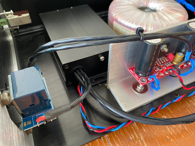
So in this post I will make another PCM56 DAC. Same schematic but lots of improvement especially in the power supply section. I will put this DAC inside my Gainclone amplifier here and this will become an integrated amplifier.
In this DAC build, I make so much improvement over the design. This would become more compact in size to accommodate all sections in this DAC required.
To start with this project, I firstly draw a components placement exactly the same as the board that I trying to use. This help me a lot to determined the components position, so they will neat arranged.
I will build this DAC by point-to-point connection, so the effective components placement is very important to make those components arrangement in line with the schematic. This also help to determine every components size correspondence to the size of the board.
The board is custom cutting same as the aluminum casing use here. The size of the casing is 11 cm x 7 cm x 3.5 cm. This casing is also a heat sink for the voltage regulator IC to dissipate the heat.
After all components on hand, then I start to populating all of them one by one.
From the photos above you can see all components from digital receiver, channel splitter, dual DAC and LPF circuit is already on board. This more compact than the first time I built this DAC.
In this build, I using LM317 and LM337 as voltage regulator instead of fixed regulator like previous built. This LM317 and LM337 has better ripple rejection compares to the fixed one. This ripple rejection numbers is very important since I will using the same power supply source taken from the amplifier board.
Using this kind regulators has the drawback. It's require additional components such as resistors, diodes and capacitors to make they works as per specification. This will require more PCB space to accommodate those additional components. The schematic for this voltage regulator is provided on their datasheet.
The plus point with this regulators, I can adjust the voltage output. In this build, the output voltage will be set +10 volt and - 10 volt. Much higher than the previous built, but still within the DAC IC specification.
After all components are installed on the board, then the next step is put it inside the casing. I also measure the casing for making a holes for the input output cable and for the regulator IC.
The regulator should not attach directly to the casing. To avoid this, I using an isolator. This isolator also act as heat transfer from the IC's to the casing.
The next step is attaching the SPDIF input cable, DC voltage cable and line out cable.
As an integrated amplifier, ideally I should put a switch before the volume control. This switch function is for selecting the input between analog input or digital input of the DAC module. But I will save this project for later. Right now the digital SPDIF input is the only input available for this amplifier.
So it is all the steps I made for this second built PCM56 DAC. It is finished and the sound is wonderful.
Disclaimer: Any statement and photos in this article are not allowed to copy or publish without written permission from the writer. Any injury or loss from following tips in this article is not under writer responsibility.


Comments
Post a Comment